| XFAB 350 nm – Brazil IP (2012) | |
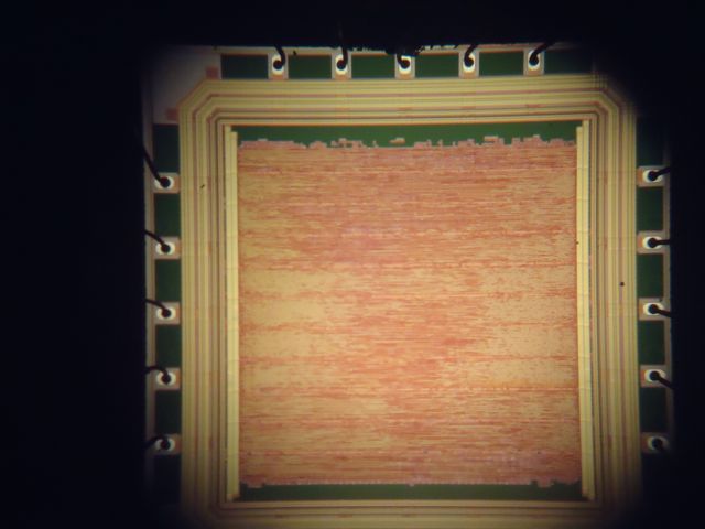  |
This chip was designed by the GAMA team for the Brazil-IP project. It contains a 32-bit floating-point unit and includes a serial interface for in/out communication. The operating frequency is 16 MHz and the hole circuit is composed of 150.000 transistors.
Area: 3mm x 3mm |
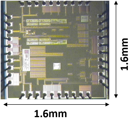
| TSMC 180 nm – FreeMiniasic IMEC/Europractice (2015) | |
 |
This IC was designed in collaboration with the Integrable System Laboratory (LSI) of the University of São Paulo – USP. It is composed of the following circuits:
|
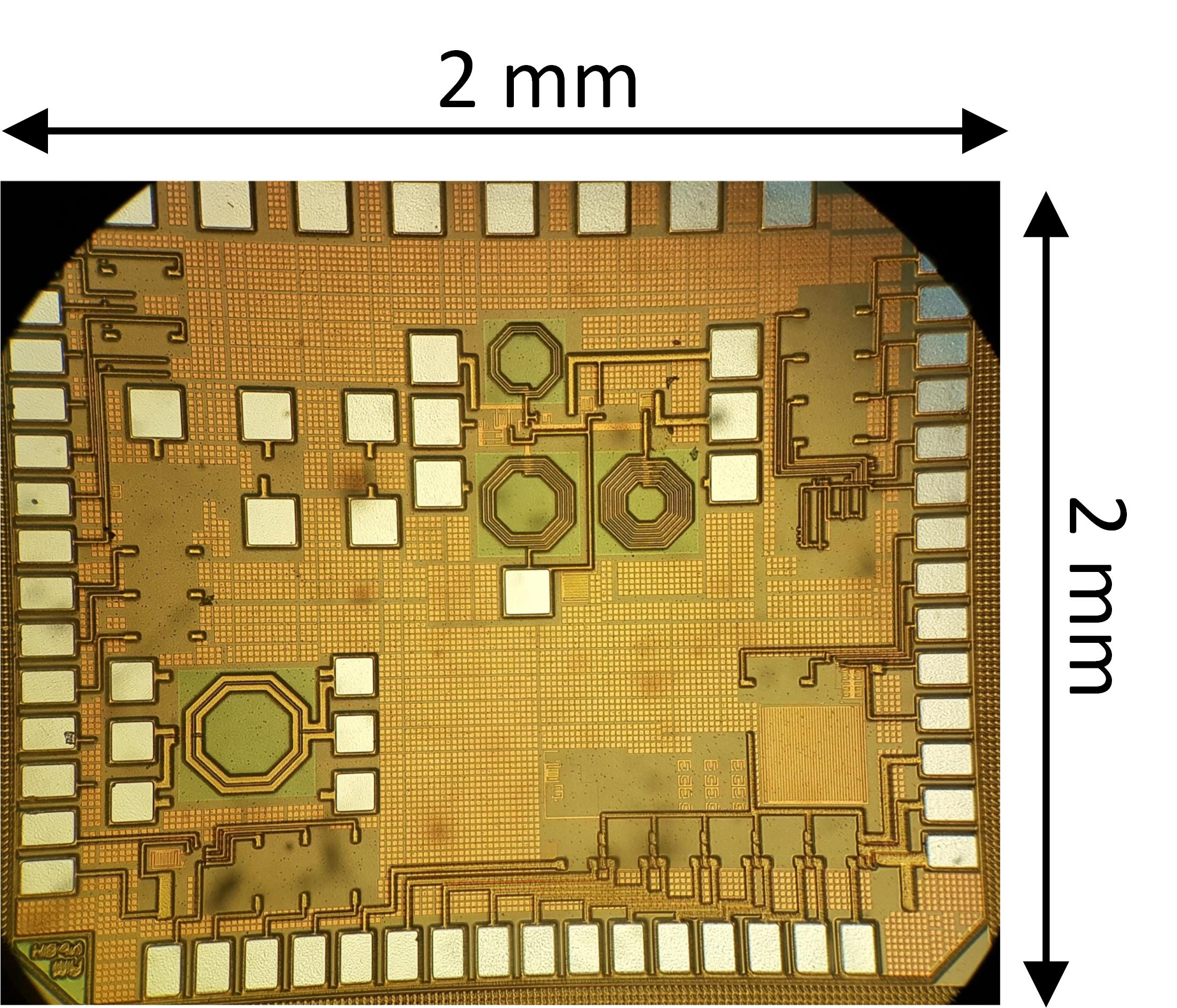
| TSMC 130 nm – IMEC/Europractice/CERN (2015) | |
 |
This IC was designed in collaboration with the Integrable System Laboratory (LSI) of the University of São Paulo – USP using some free silicon area of the SAMPA chip used at CERN by the ALICE (A Large Ion Collider Experiment). It is composed of the following circuits:
|
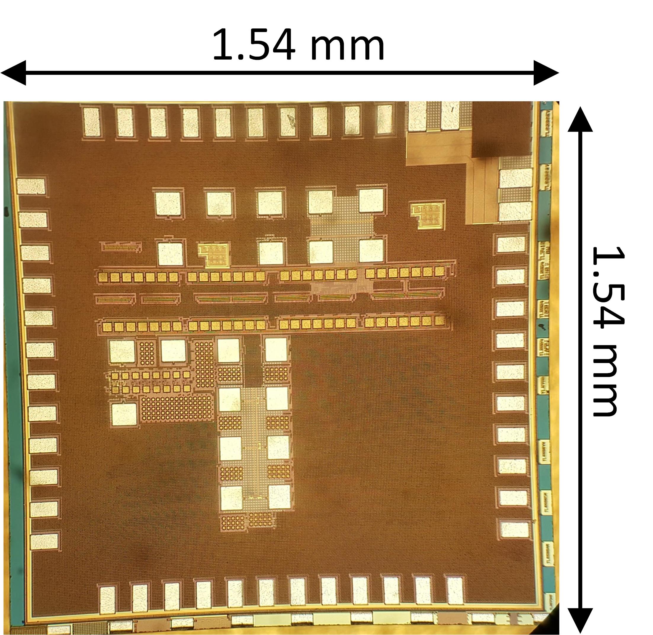
| Global Foundries 130 nm – MOSIS (2016) | |
 |
This IC was designed in collaboration with the Federal University of Rio Grande do Sul. It is composed of the following circuits:
|
| TSMC 180 nm – FreeMiniasic IMEC/Europractice (2016) | |
 |
This IC is composed of the following circuits:
|
| TSMC 180 nm – FreeMiniasic IMEC/Europractice (2017) | |
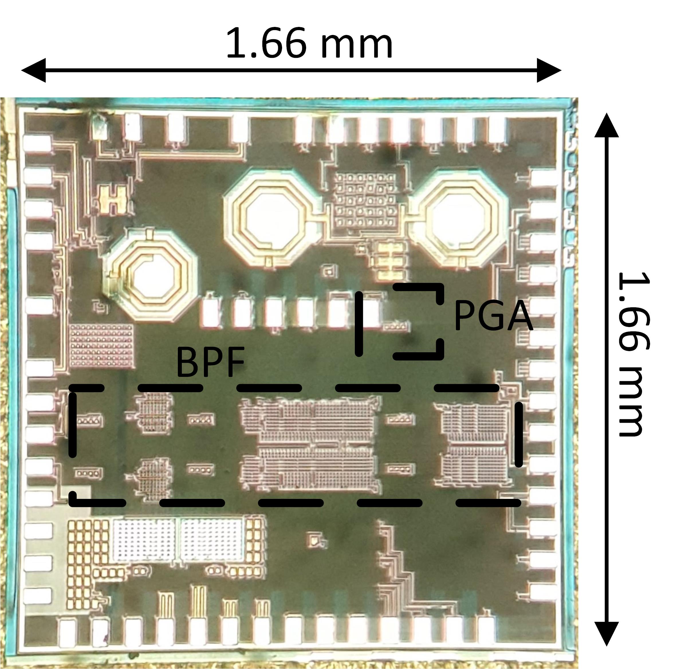 |
This IC was designed in collaboration with the Integrable System Laboratory (LSI) of the University of São Paulo – USP.
Some of the front-end circuits of a Bluetooth Low Energy RF receivers were prototyped in this IC:
|
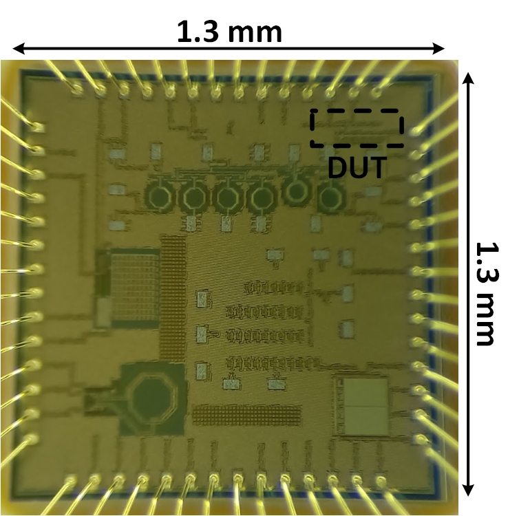
| Global Foundries 130 nm – MOSIS (2018) | |
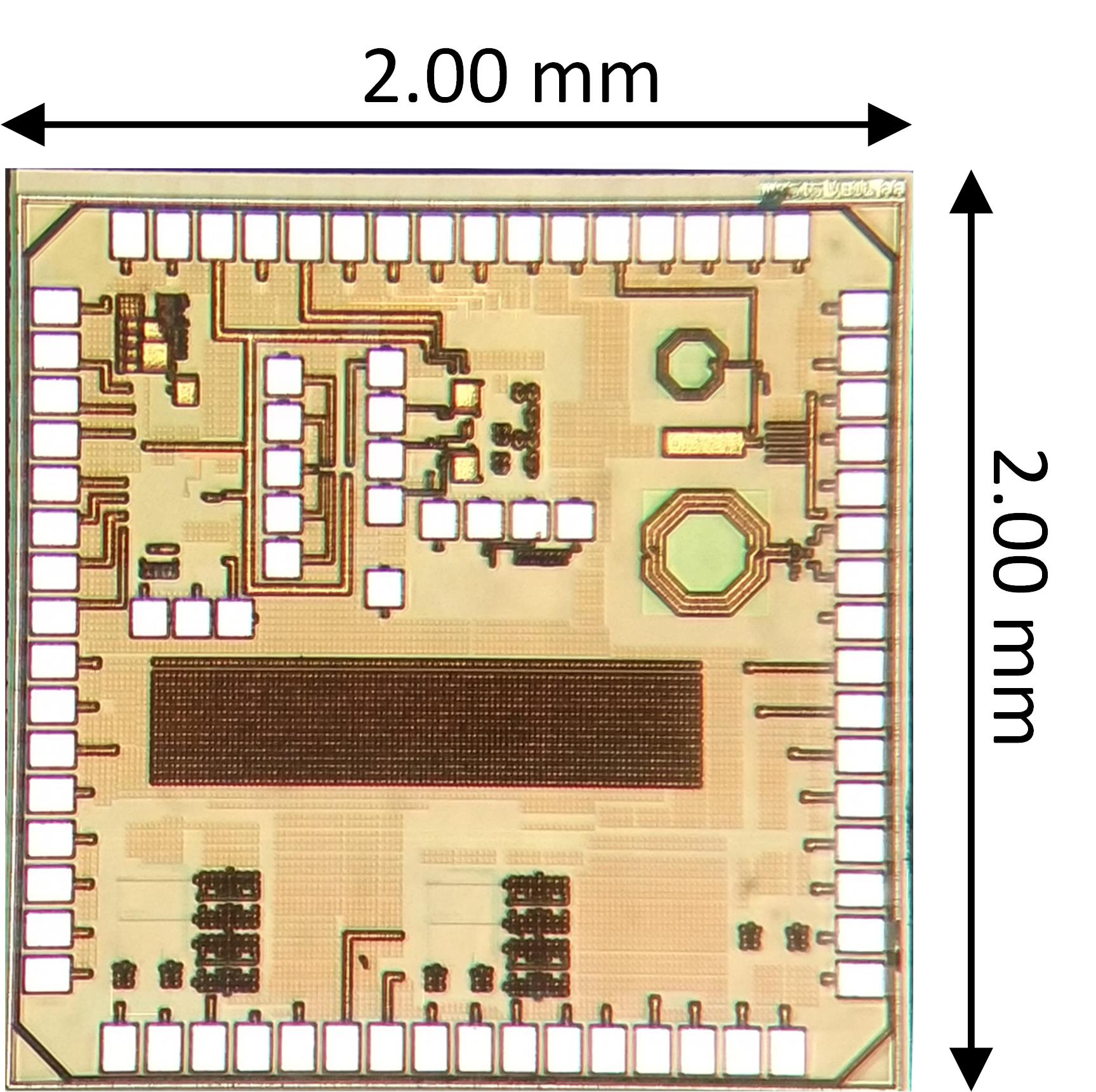 |
This IC was designed in collaboration with the Integrable System Laboratory (LSI) of the University of São Paulo – USP.
Some of the front-end circuits of a Bluetooth Low Energy RF receivers were prototyped in this IC:
|
| TSMC 180 nm – FreeMiniasic IMEC/Europractice (2018) | |
 |
This IC is composed of some active filters and sigma-delta analog to digital converters. All the circuits are able to operate with ultra-low voltage supplies (<0.6V) and are targeted to IoT applications |
| TSMC 180 nm – FreeMiniasic IMEC/Europractice (2021) | |
 |
This IC was design by the DMPSV group od the University of São Paulo as a part of the project of breast cancer detections by meas of UWB RF signals. The GAMA team has designed some blocks of this IC. In this case a negative-resistance based amplifier was prototyped in this IC. |